For over a hundred years the analog dog wagged the digital tail. The effort to extend the reach of our senses – sight, hearing, even (after a manner of speaking) touch, drove engineers and scientists to search for better components for telegraph, telephone, radio and radar equipment. It was a happy accident that this also opened the door to new kinds of digital machines.1 I set out to tell the story of this repeated exaptation, whereby telecommunications engineers supplied the raw materials of the first digital computers, and sometimes even designed and built such computers themselves.
By the 1960s, however, this fruitful relationship came to a close, and so too does my story. The makers of digital equipment no longer had any need to look outward to the world of the telegraph, telephone, and radio for new and improved switches, because the transistor itself provided a seemingly inexhaustible vein of improvements to mine. Year after year, they dug deeper and deeper, always finding ways to exponentially increase speed and reduce costs.
None of this, however, would have happened, if the invention of the transistor had stopped with Bardeen and Brattain.
A Slow Start
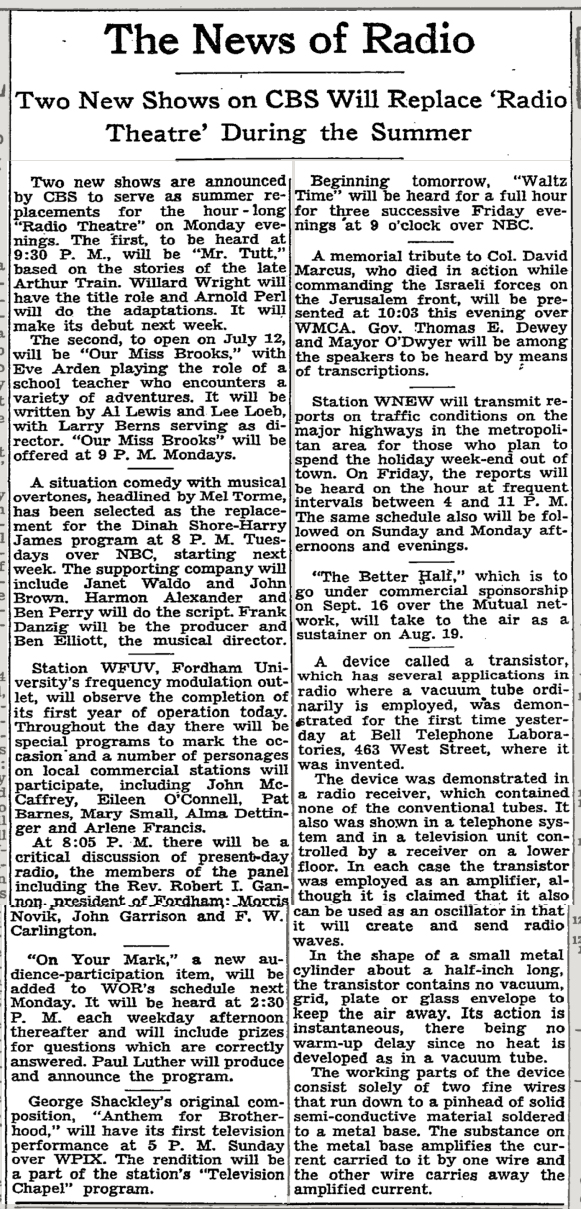
The popular press did not react to Bell Labs’ announcement of the transistor with great enthusiasm. On July 1, 1948, The New York Times gave it three paragraphs at the bottom of their “The News of Radio” bulletin. The notice appeared after several other announcements evidently deemed more significant: touting, for example, the one-hour “Waltz Time” broadcast coming to NBC. Hindsight tempts us to mock, or even scold, the ignorance of the anonymous authors – how did they fail to recognize the world-shaking event that had just transpired?
But hindsight distorts, amplifying the few signals that we now know to be significant, though at the time they were lost in a sea of noise. The transistor of 1948 was very different from the transistors in the computer on which you are reading this2. So different that, despite their common name and the unbroken line of ancestry that connects them, they should be considered a different species of thing, if not a different genus. They share neither material composition, nor structural form, nor functional principles; not to mention their tremendous difference in size. Only by being reinvented again and again did the clunky device constructed by Bardeen and Brattain become capable of transforming the world and the way we live in it.
In truth, the germanium point-contact transistor deserved no more attention than it got. It suffered from a number of defects relative to its vacuum tube cousin. To be sure, it was rather smaller than even the most compact tube. Its lack of a heated filament meant it generated less heat, consumed less power, would not burn out, and required no warming up before it could be used.
But the accumulation of dirt on the contact surface led to failures and undermined its potential for longer life; it produced a noisier signal; worked only at low power and in a narrow frequency band; failed when exposed to heat, cold or humidity; and could not be produced uniformly. A sequence of transistors all constructed in the same way by the same people would differ obnoxiously in their electrical characteristics. All of this baggage came at a retail price some eight times higher than that of a typical tube.
Not until 1952 did Bell (and other patent licensees) work out the manufacturing kinks sufficiently for point-contact transistors to see real use, and even so they never spread much beyond the hearing aid market, where price sensitivity was relatively low, and the advantages offered in battery life dominated other considerations.3
The first efforts to remake the transistor into something better and more useful, however, had already begun. In fact, they began well before the public even learned that the transistor existed.
Shockley’s Ambition
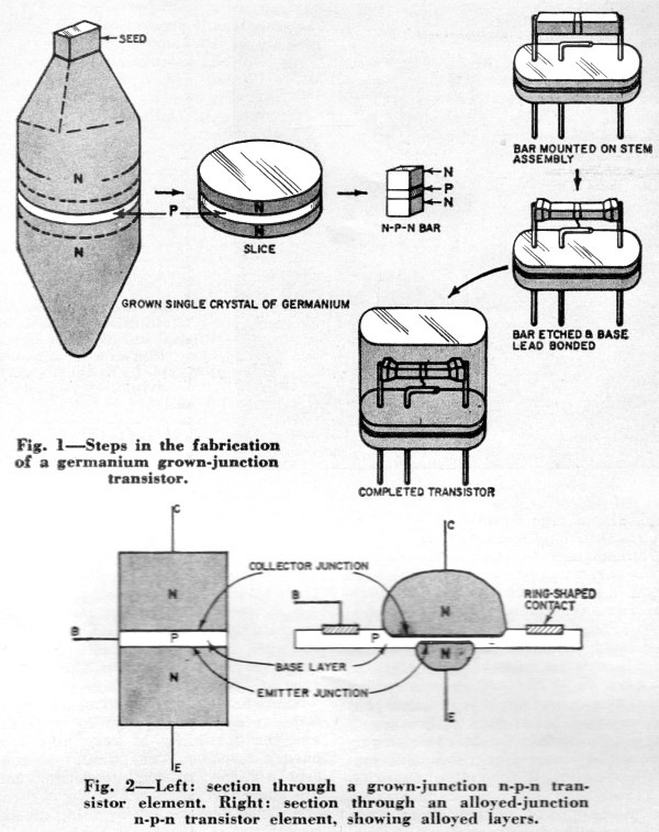
As the year 1947 came to a close, an agitated Bill Shockley took a business trip to Chicago. He had some vague ideas about how to trump Bardeen and Brattain’s recently invented transistor, but he had not yet had the chance to develop them. And so, rather than enjoy his time off between business engagements, he spent New Year’s Eve and New Year’s Day in his hotel room, scribbling out some twenty pages of notes on his ideas. Among them was a proposal for a new kind of transistor consisting of a kind of semiconductor sandwich – a slice of p-type germanium between two pieces of n-type.
Emboldened by this ace in his back pocket, Shockley then confronted Bardeen and Brattain on his return to Murray Hill, claiming full credit for the invention of the transistor. Had it not been his field-effect idea that had sent Bardeen and Brattain scurrying off to the lab? Should not the authorship of the patent thus fall entirely to him? But Shockley’s stratagem backfired: Bell Labs patent lawyers found that an obscure inventor, Julius Lilienfeld, had patented a field-effect semiconductor amplifier almost twenty years prior, in 1930. Lilienfeld had surely never built the thing he proposed, given the state of materials science at the time, but the risk of an interference proceeding was too great – better to avoid mentioning the field effect in the patent altogether.
So, though Bell Labs would allow Shockley a generous share of the public credit, it named only Bardeen and Brattain in the patent. The damage was done, however: Shockley’s ambition destroyed his relationship with his two subordinates. Bardeen abandoned the transistor, and shifted his focus to superconductivity. He left Bell Labs in 1951. Brattain remained but refused to work with Shockley again, and insisted on being transfered to another group.
His inability to get along with others made it impossible for Shockley to rise any further at Bell Labs, and so he too jumped ship. In 1956, he returned home to Palo Alto to found his own transistor manufacturing company, Shockley Semiconductor. Before leaving for the West Coast, he left his wife Jean, while she was recovering from uterine cancer, for his soon-to-be second wife, Emmy Lanning. But of the two halves of his California dream — new company and new wife — only one would last. In 1957, Shockley’s best engineers, irritated by his management style and the direction in which he was taking the company, defected to form a new firm called Fairchild Semiconductor.

So Shockley abandoned the hollowed-out husk of his company to take a position in the electrical engineering department at Stanford. There he proceeded to alienate his colleagues (and his oldest friend, physicist Fred Seitz) with his newfound interest in dysgenics and racial hygiene – unpopular topics in the United States since the late war, especially so in academia. He delighted in stirring up controversy, riling up the media, and drawing protesters. He died in 1989, alienated from his children and his peers, attended only by his eternally devoted second wife, Emmy.
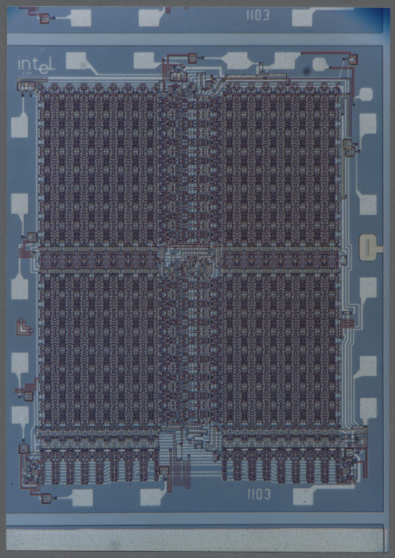
Though his own attempt at entrepreneurship had failed miserably, Shockley had cast seed onto fertile ground. The San Francisco Bay area teemed with small electronics firms and had been irrigated with funds from the federal government during the war. Fairchild Semiconductor, Shockley’s accidental offspring, itself spawned dozens of new firms, among them two names still very well-known today: Intel and Advanced Micro Devices (AMD). By the early 1970s, the area had acquired the moniker “Silicon Valley.” But wait – Bardeen and Brattain had built a germanium transistor. Where did the silicon come from?

To The Silicon Junction
The new kind of transistor that Shockley devised in his Chicago hotel had a happier destiny than that of its inventor. This was thanks to one man’s determination to grow single, pure semiconductor crystals. Gordon Teal, a physical chemist from Texas who had studied the then-useless element of germanium for his doctoral thesis, had joined Bell Labs in the thirties. After learning about the transistor, he became convinced that its reliability and power could be vastly improved by crafting it from a pure monocrystal, rather than the polycrystalline aggregates then being used. Shockley discouraged this effort, believing that it was an unnecessary waste of resources.
But Teal persevered, and succeeded, with the help of a mechanical engineer named John Little, in constructing an apparatus that pulled a tiny seed crystal from a molten bath of germanium. As the germanium cooled around the seed, it extended its crystalline structure, drawing out a continuous, and almost entirely pure, semiconductor lattice. By the spring of 1949 Teal and Little could produce crystals on demand, and tests showed that they vastly outperformed their poly-crystalline counterparts. In particular, injected minority carriers could survive inside them for one hundred microseconds or more (versus ten microseconds or less in other crystal samples).4
Teal could now avail himself of more resources, and recruited more men to his team, among them another physical chemist who came to Bell Labs by way of Texas, Morgan Sparks.5 They began altering the melt to make p-type or n-type germanium by adding pellets of the appropriate doping agents. Within another year they had refined their technique to the point that they could actually grow an n-p-n germanium sandwich right out of the melt. And it worked just as Shockley had predicted: an electrical signal on the p-type material modulated the flow of electricity between two other leads attached to the n-type slices that surrounded it.
This grown-junction transistor outclassed its point-contact predecessor in almost every dimension. Most notably they were more reliable and predictable, far less noisy (and thus more sensitive), and extremely power efficient – drawing one million times less power than a typical vacuum tube.6 In July 1951, Bell Labs held another press conference to announce this new creation. Before the original transistor had even gotten off the ground commercially, it had already been rendered largely irrelevant.
Yet it was still only the beginning. In 1952, General Electric (GE) announced a new process for making junction transistors called the alloy-junction method. This involved melting two pellets of indium (a p-type donor) into either side of a thin slice n-type germanium. The process was simpler and less expensive than growing junctions out of the melt, generated less resistance, and supported higher frequencies.
The following year Gordon Teal decided to return to his home state, and took a job at Texas Instruments (TI), in Dallas. Founded as Geophysical Services, Inc., a maker of oil prospecting equipment, TI branched out into electronics during the war and was now entering the transistor market under a license from Western Electric (Bell’s manufacturing arm).
Teal brought with him the newest set of skills he had developed at Bell Labs: the ability to grow and dope monocrystals of silicon. Germanium’s most obvious weakness was its sensitivity to temperature. When exposed to heat, the germanium atoms in the crystal rapidly shed free electrons, becoming more and more like a pure conductor. At around 170 degrees Farenheit, they ceased to work as transistors altogether. The military – a potential customer with little price sensitivity and a powerful need for stable, reliable and small electronic components – was a prime target for transistor sales. But temperature-sensitive germanium would not do for many military applications, especially in aerospace equipment.
Silicon was much more stable, but this came at the price of a much higher melting point, as high as that of steel. This created great difficulties given that pure crystals were needed to make high quality transistors. The hot molten silicon would leach impurities from whatever crucible it rested in. Teal and his team at TI managed to overcome these difficulties, with the help of ultra-high purity silicon samples from DuPont. In May 1954, at an Institute of Radio Engineers conference in Dayton, Ohio, Teal demonstrated that the new silicon devices coming out of his lab continued to amplify even when immersed in hot oil.7
The Upstarts
At last, some seven years after the initial invention of the transistor, it could be made from the material with which it has become synonymous. As much time again would pass before transistors appeared that roughly resemble the form of those in our microprocessors and memory chips.
In 1955, Bell Labs scientists succeeded in making silicon transistors with a new doping technique – rather than adding solid dopant pellents to liquid melt, they diffused vaporized dopants into a solid semiconductor surface. By carefully controlling the temperature, pressure and duration of exposure, they achieved exactly the desired depth and amount of doping. This more precise control of the manufacturing process resulted in a more precise control over the electrical properties of the end product. Just as importantly, the diffusion technique opened the doors to batch production – one could dope a large slab of silicon all at once and then slice it up into transistors after the fact. The military provided the cash needed to offset Bell’s high up-front costs for setting up manufacturing. They wanted the new product for the ultra-high-frequency Distant Early Warning Line, a chain of arctic radar stations designed to detect Soviet bombers coming over the North Pole, and were willing to pay $100 per transistor.8
Doping, combined with photolithography to control the placement of the dopants, made it possible to imagine etching a complete circuit in one semiconductor wafer, an achievement which was realized independently at Fairchild Semiconductor and Texas Instruments in 1959. Fairchild’s “planar process” used the chemical deposition of metal films to connect the transistor’s electrical contacts. This obviated the need for hand wiring, simultaneously reducing costs and increasing reliability.
Finally, in 1960, two Bell Lab engineers (John Atalla and Dawon Kahng) realized Shockley’s original concept for a field-effect transistor. A thin layer of oxide on the semiconductor surface proved highly effective at suppressing the surface states, allowing the electric field from an aluminum gate to pass into the body of the silicon. This was the origin of the MOSFET (metal-oxide semiconductor field-effect transistor), which proved so amenable to miniaturization and still features in almost all computers today.9 Here at last, thirteen years after the initial invention of the transistor, is something recognizably like the transistor in your computer. It was simpler to make and used less power than junction transistors, but was a laggard in responding to signals. Not until the advent of large-scale integration circuits with hundreds or thousands of components on a single chip did the advantages of field-effect transistors come to the fore.

The field-effect proved to be the last major contribution by Bell Labs to the development of the transistor. The large electronics incumbents such as Bell (via Western Electric), General Electric, Sylvania, and Westinghouse developed an impressive record of semiconductor research. From 1952-1965, Bell Labs alone secured well over two hundred patents in the field. Nonetheless the commercial marketplace rapidly passed into the hands of new players like Texas Instruments, Transitron and Fairchild.
The early market for transistors was simply too small for the big incumbents to pay much attention to: roughly $18 million a year in the mid-1950s, versus over $2 billion for the electronics market as a whole. Meanwhile, though, the research labs of those same incumbents served as unwitting training facilities, where young scientists could soak up knowledge about semiconductors before moving on to sell their services to smaller firms. By the time the market for tube electronics began to decline seriously, in the mid-1960s, it was far too late for Bell, Westinghouse and the like to overtake the upstarts.10
The Computer Transistorized
There were four notable areas where transistors made significant inroads in the 1950s. The first two were hearing aids and portable radios, where lower power consumption (and thus longer battery life) trumped other considerations. The U.S. military was the third. They had high hopes for transistors as rugged and compact components in everything from field radios to ballistic rockets. But in the early years their spending on transistors was more of a bet on the future of the technology than an indication of its present value. And, finally, there was digital computing.
In the case of the computer, the severe disadvantages of vacuum tube switches were well known, so much so that many skeptics before the war had believed that an electronic computer could never be made practical. When assembled in units of thousands, tubes devoured electrical power while generating vast amounts of heat, and could be relied on only to burn out regularly. Thus the power-sipping, cool, and filament-less transistor appeared as a kind of savior to computer manufacturers. Its disadvantages as an amplifier (such as a noisier output signal) presented much less of a problem when used as a switch. The only real obstacle was cost, and that would began to fall precipitously, in due time.
All of the early American experiments in transistorized computers occurred at the intersection of the desire of the military to explore the potential of a promising new technology, and the desire of computer engineers to migrate to a new, better kind of switch.
Bell Labs built the TRADIC in 1954 for the U.S. Air Force, to see if transistors would make it possible to send a digital computer on-board a bomber, to replace analog navigation and bomb-sighting aids. MIT’s Lincoln Laboratory, developed the TX-0 computer as part of its vast air-defense system project, in 1956. The machine used yet another transistor variant, the surface-barrier transistor, which was well suited to high-speed computing. Philco built its SOLO computer under Navy contract (but really on behalf of the National Security Agency), completing the work in 1958. (It was another surface-barrier design.)
The story in Western Europe, which was not so flush with Cold War military resources, was rather different. Machines like the Manchester Transistor Computer, Harwell CADET (another ENIAC-inspired name, obscured by mirror-writing), and Austrian Mailüfterl were side projects, using whatever resources the creators could scrape together -including first-generation point-contact transistors.
There is much jockeying among these various projects for the title of first transistorized computer. It all, of course, depends on which definitions one chooses for “first”, “transistorized,” and “computer.” We know where the story ends up in any case. The commercialization of transistorized computers followed almost immediately. Year-by-year computers of the same price grew ever more powerful while computers of the same power fell ever lower in price, in a process so seemingly inexorable that it became enshrined as a “law”, to sit alongside gravity and the conservation of matter. Shall we quibble over which was the first pebble in the avalanche?
Why Moore’s Law?
As we reach the close of our story of the switch, it is worth asking the question: What did cause this avalanche? Why does11 Moore’s Law exist? There is no Moore’s Law of airplanes or vacuum cleaners, nor, for that matter, of vacuum tubes or relays.
There are two parts to the answer:
- The logical properties of the switch as a category of artifact
- The ability to use entirely chemical processes to make transistors
First, the essence of the switch. The properties of most artifacts must satisfy a wide variety of non-negotiable physical constraints. A passenger airplane must be able to hold up the combined weight of many people. A vacuum cleaner must be able to pull up a certain amount of dirt in a given amount of time, over a given physical area. Neither airplanes nor vacuum cleaners would be useful if reduced to nanoscale.
On the other hand, a switch – an automatic switch, one never touched by human hands – has very few physical constraints. It needs to have two distinguishable states, and it needs to be able to tell other switches like itself to change between those states. That is to say, all it needs to do is to turn on, and turn back off again. Given this, what is special about transistors? Why have other kinds of digital switch not seen such exponential improvements?
Here we come to the second fact. Transistors can be made using chemical processes with no mechanical intervention. From the beginning, the core element of transistor manufacturing was the application of chemical dopants. Then came the planar process, which removed the last mechanical step in the manufacturing process – the attachment of wires. It thus cast off the last physical constraint on miniaturization. No longer did transistors need to be large enough for fingers – or a mechanical device of any sort – to handle. Mere chemistry would do the job, at an unimaginably tiny scale: acids to etch, light to control which parts of the surface will resist the etching, and vapors to deposit dopants and metal films into the etched corridors.
Why miniaturize in the first place? Decreased size brought with it an array of pleasant side-effects: higher switching speeds, reduced power consumption, and lower unit costs. Therefore powerful incentives drove everyone in the business to look for ways to make their switches ever smaller. And so the semiconductor industry, within a human lifetime, went from making switches the size of a fingernail to packing tens of millions of switches within a single square millimeter. From asking eight dollars a switch to offering twenty million switches per dollar.

Further Reading
Ernest Bruan and Stuart MacDonald, Revolution in Miniature (1978)
Michael Riordan and Lillian Hoddeson, Crystal Fire (1997)
Joel Shurkin, Broken Genius (1997)
- To make a switch from an amplifier, one need only ignore all the complexity of the output waveform, and treat a certain output level as “off” and another as “on”. ↩
- Yes, okay, it’s possible that you printed it out. ↩
- After 1954, Bell waived transistor licensing fees for hearing aids, in honor of Alexander Graham Bell’s work on behalf of the deaf. ↩
- Riordan and Hoddeson, 173-179. ↩
- Though born in Colorado, Sparks grew up in Texas, and earned a bachelor’s and master’s degree in chemistry at Rice University. ↩
- Riordan and Hoddeson, 193. ↩
- Riordan and Hoddeson, 208-210. None of the sources that I’ve found explain to my satisfaction how the TI engineers overcame the limitations of silicon where others had failed, other than the deus ex machina of extra-pure silicon from Du Pont, which just regresses the problem one step – how did Du Pont make such pure silicon? ↩
- Riordan and Hoddeson, 224; Bruan and MacDonald, 63. This was at a time when a new car could be had for $2000. ↩
- The MOSFET invention is significant in another way, given that Atalla was born in Egypt and Kahng in South Korea – virtually the only figures in our story so far not of European descent. ↩
- Braun and MacDonald, 60-64. This has a slight ring of Clayton Christensen’s Innovator’s Dilemma, although it differs from most of the case studies he presents, in which the disruption comes from the bottom of the market. The transistor, by contrast, was a high-end and very expensive component whose biggest market was in aerospace. ↩
- Or “did”. Much ink could be spilled on whether, when, and why Moore’s Law has ended. Another time, perhaps. ↩

I hope you will continue writing as I’ve enjoyed your posts very much!
LikeLike
[…] https://technicshistory.wordpress.com/2018/03/31/the-transistor-part-3-endless-reinvention/ […]
LikeLike
[…] [Previous part] [Next part] […]
LikeLike
Again, a marvelous experience to read the article.
I am eager to read the further articles in the next series.
Real learning.
Thanks again.
LikeLike
Thank you, I’m glad you enjoyed the work.
LikeLike
Reblogged this on josephdung.
LikeLike
[…] How the transistor came to be […]
LikeLike
Very good perspective, from the telegraph key to the actual elctronic circuits. I just finished reading the book and I hadnt idea about all the actors involved on the evolution of electronics, particularly semiconductors.
Tks again for the book!!
LikeLike