The crucible of war prepared the ground for the transistor. The state of technical knowledge about semiconductor devices advanced enormously from 1939 to 1945. There was one simple reason: radar. The single most important technology of the war, its applications included detecting incoming air raids, locating submarines, guiding nightfighters to their targets, and aiming anti-aircraft guns and naval cannon. Engineers even managed to pack tiny radar sets inside of artillery shells, to make them detonate when they passed near a target – the proximity fuse. The origins of this potent new military technology, however, lay in a much more peaceful domain: the scientific exploration of the upper atmosphere.
Radar
In 1901, the Marconi Wireless Telegraph Company succeeded in sending a wireless message across the Atlantic, from Cornwall to Newfoundland. This was a fact confounding to modern science. If radio transmissions traveled in straight lines (as they certainly ought to) this feat should have been impossible. There is no straight line between England and Canada that does not cross through the Earth, so Marconi’s message should have continued right on into outer space. American engineer Arthur Kennelly and British physicist Oliver Heaviside both independently hypothesized that the explanation must lay in a layer of ionized gas in the upper atmosphere, capable of reflecting radio waves back down towards Earth.1
By the 1920s, scientists had developed new equipment first to prove the existence of this ionosphere, then to probe its structure. They used vacuum tubes to generate shortwave radio pulses, shaped antennas to direct them up into the atmosphere and register their echoes, and cathode ray tubes to display the results. The longer the delay until the echo returned, the farther away the ionosphere must be. The technique was known as ionospheric sounding, and it provided the basic technical infrastructure required for radar2.
It was only a matter of time for those with the right knowledge, resources, and motivation to realize the potential terrestrial applications of such equipment3. This became increasingly likely as radio grew more and more commonplace, and more and more people noticed signal interference from nearby ships, aircraft, and other large objects. Knowledge of the techniques for probing the upper atmosphere spread during the second International Polar Year (1932-1933), which included a project to map the ionosphere from various stations in the Arctic. Shortly thereafter teams in Britain, the U.S., Germany, Italy, the Soviet Union, and elsewhere all developed basic radar systems.4

Then came war, and with it the importance of radar to the state – and thus the resources available to develop it – increased sharply. In the United States, these resources coalesced around a new organization founded in 1940 at the Massachusetts Institute of Technology (MIT) known as the “Rad Lab”5. Though less famous in later years than the Manhattan Project, the Rad Lab recruited equally exceptional physics talents from across the United States. Five of the early recruits (who included Luis Alvarez and I. I. Rabi) would go on to win Nobel prizes.6 By end of war the lab had about 500 Ph.D. scientists and engineers, out of a total of almost 4,000 employees. Half a million dollars – as much as the entire budget for ENIAC – was spent on the “Radiation Laboratory Series” alone. It consisted of twenty-seven volumes that captured and disseminated the knowledge gained at the lab during the war.7

One major area of research for the Rad Lab was high-frequency radar. Early radars all transmitted in wavelengths measured in meters. But higher-frequency beams, with wavelengths measured in centimeters – microwaves – would have more compact antennas, and disperse less over long distances, offering huge advantages in range and precision. Microwave radars would be able to fit in the nose of a plane, and detect objects as small as a submarine periscope.
First to crack the problem were a team of British physicists at the University of Birmingham. In 1940, they developed a device they called the cavity magnetron, which acted as a kind of electromagnetic “whistle,” turning an incoherent blast of electricity into a powerful and precisely tuned beam of microwaves8. This was a microwave transmitter a thousand times more powerful than its next closest competitor; it unlocked the door to practical high-frequency radar transmitters. But such a transmitter would need a companion, a receiver capable of registering high-frequencies. Here we rejoin the story of semiconductors.
The Second Coming of the Cat’s Whisker
For it turned out that vacuum tubes were not at all well suited for receiving microwave radar signals. The gap between hot cathode and cold anode creates capacitance, which causes the circuit to fail at high frequencies. The best available technology for high-frequency radar was the old-fashioned cat’s whisker – a little twist of wire pressed into a semiconductor crystal. This fact was discovered independently in several places, but most relevant to our story were the events that took place in New Jersey.
In 1938, Bell Labs received a contract from the Navy to develop a fire-control radar in the forty-centimeter range – a much shorter wavelength, and thus higher frequency, than the existing state of the art in this pre-cavity magnetron era. The main research work for the project was assigned to the Bell Labs branch in Holmdel, due south of Staten Island. It did not take the researchers there long to realize what they needed for their high-frequency receiver, and soon engineer George Southworth was rummaging through radio shops in Manhattan to find an old cat’s whisker detector. As expected, it worked much better than a tube-based receiver, but the results were inconsistent. So Southworth sought out an electrochemist named Russel Ohl, and asked him to try to improve the uniformity of response from point-contact crystal detectors.
Ohl was an unusual character who believed himself a figure of technical destiny, receiving periodic flashes or visions of things to come. For example, he claims to have known since 1939 that a silicon amplifier would be invented, but that he would not be fated to invent it. After studying dozens of options, he settled on silicon as the best material for Southworth’s receivers. The problem was to control its content so that he could control its electrical properties. Industrial silicon ingots were commonplace, being used in steel mills to strengthen the metal, but the mills hardly cared if the silicon contained, say, 1% phosphorus. So, with the help of a pair of metallurgists Ohl set out to render much purer ingots than any had ever before attempted.
As they worked, his team discovered that some of their crystal samples rectified in one direction, and some in the other: they dubbed these “n-type” and “p-type.” Further analysis suggested that different impurities were responsible for each. Silicon sits in the fourth column of the periodic table, meaning it has four electrons in its outermost shell. In an ingot of perfectly pure silicon, each of those four electrons would bond with a neighbor. Impurities from the third column, such as boron, which had one fewer electron to share, created a “hole,” an extra space where current could move within the crystalline structure. This resulted in a p-type semiconductor (with an excess of positive carriers). Elements from the fifth column, such as phosphorus, supplied extra free electrons for carrying current, creating an n-type semiconductor.

All of this research was quite fascinating, yet by 1940 Southworth and Ohl were not much closer to a working high-frequency radar set than when they started. The British, meanwhile, pressed for immediate practical results by the looming threat of the Luftwaffe, had already created production-ready microwave-range detectors to pair with their magnetron-based transmitters.
The balance of technical achievement would soon tip to the western side of the Atlantic, however. For Churchill decided to reveal all of Britain’s technical secrets to the Americans, even before they entered the war as full belligerents (as he assumed they, eventually, must do). He felt the risk of a leak worthwhile, balanced against the chance of bringing the full industrial might of the United States to bear on problems like atomic weaponry and radar. The British Technical and Scientific Mission (more popularly known as the Tizard Mission) arrived in Washington in September 1940, carrying among its baggage a bounty of technical wonders.
The revelation of the extraordinary power of the cavity magnetron, and the effectiveness of British crystal detectors at receiving the resulting signals, galvanized the American effort on semiconductors, in support of high-frequency radar. There was a great deal of work to do, mostly in the realm of materials science. To meet the scale of demand, semiconductor crystals “had to be produced by the millions in far higher quality than previously available. Rectification needed to be improved, vulnerability to shock and burnout reduced, and variations between batches of crystal minimized.”9

The Rad Lab opened new research departments to investigate the properties of semiconductor crystals and how they could be altered to maximize their value as receivers. Silicon and germanium were the most promising materials, so the Rad Lab hedged its bets and launched an adjunct research program to study each: silicon at Penn, and germanium at Purdue. Industrial giants Bell, Westinghouse, Du Pont, and Sylvania started their own semiconductor research programs, and also began working up new production lines for crystal detectors.
These combined efforts brought the purity standard of silicon and germanium crystals from 99% at the start of the war up to 99.999% at the end – only one impurity in every 100,000 atoms. In the process, a substantial cadre of scientists and engineers acquired intimate familiarity with both the abstract properties of germanium and silicon and the concrete techniques needed to manipulate their composition: melting them, growing them into crystals, and doping them with tightly controlled doses of impurities (such as boron, which was shown to improve conductivity).10
Then the war ended. The demand for radar equipment disappeared, but the knowledge and skills acquired during the war did not, and the dream of a solid state amplifier had not been forgotten. The race would now be on to build one. At least three teams were well-positioned to claim the prize.
West Lafayette
First, at Purdue University, was the group under an Austrian-born physicist named Karl Lark-Horovitz. His talent and influence had single-handedly brought Purdue’s physics department out of obscurity, and accounts for the Rad Lab’s decision to center their germanium research at his lab.
By the early 1940s, silicon was considered clearly the best material for radar rectifiers, but the material just below it on the periodic table also seemed worthy of further study. Germanium had a large practical advantage over its cousin simply because its lower melting point made it so much easier to work with: about 940 degrees (Celsius), versus about 1400 for silicon – roughly the same as steel. Because of it its high melting point, it was extremely hard to make a crucible that did not bleed into the molten silicon, dirtying it.
So Lark-Horovitz and his fellow physicists spent the war studying the chemical, electrical, and physical properties of germanium. The most crucial problem to overcome was “back voltage”: germanium rectifiers would stop rectifying, allowing current to flow backwards, at very low voltages. This surge of back current would then fry other components of the radar. One of Lark-Horovitz’s graduate students, Seymour Benzer, spent over a year studying this problem, and finally came up with a tin doping mix that stopped back surges of well over one hundred volts. Shortly thereafter, Bell Lab’s manufacturing arm, Western Electric, began churning out rectifiers based on Benzer’s work for the military.
Work on germanium at Purdue continued on after the war. In June 1947, Benzer, now a professor, reported a strange anomaly: some experiments had generated high-frequency electrical oscillations within the germanium crystals. His colleague Ralph Bray, meanwhile, had continued studying “spreading resistance,” a project he began during the war. Spreading resistance described the way in which electricity flows within the germanium crystal under the point contact of the rectifier. Bray found that high-voltage pulses greatly diminished the resistance of n-type germanium to these flows. Without realizing it, he was witnessing the effect of so-called “minority” charge carriers. In n-type semiconductors, excess negative charges serve as the majority carriers, but positive “holes” could also carry current, and in this case the high-voltage pulses were tearing holes in the germanium structure, creating these minority carriers.
Bray and Benzer were tantalizingly close to a germanium amplifier, but did not realize it. Benzer cornered Bell Labs scientist Walter Brattain at a conference in January 1948 to discuss spreading resistance. He suggested to Brattain that maybe if they placed another point contact nearby the first to pick up the current, they might be able to grasp what was happening inside the surface. Brattain quietly agreed with the suggestion and walked away. As we shall see, he knew all too well what such an experiment might uncover.
Aulnay-sous-Bois
The Purdue group had both the material techniques and the grounding in theoretical physics needed to make the leap to the transistor. But they could have stumbled on it only by chance. They were interested in the physics of a material, not in pursuing a new kind of device.11 Quite different conditions obtained in Aulnay-sous-Bois, France, where two former radar researchers from Germany, Heinrich Welker and Herbert Mataré, led a team focused entirely on building semiconductor devices for industry.
Welker had first studied and then taught physics at the University of Munich, under the famed theorist Arnold Sommerfeld. From 1940 onward he abandoned the strictly theoretical and began working on radar for the Luftwaffe. Mataré (of Belgian descent), was raised in Aachen, where he studied physics. He joined the research arm of German radio giant Telefunken in 1939. During the war he moved his work east from Berlin to an abbey in Silesia to avoid Allied bombing raids, then back west to avoid the advancing Soviets, before finally falling into the hands of the American army.
Just like their counterparts in the Allied powers, the Germans knew by the early 1940s that crystal detectors were ideal radar receivers and that silicon and germanium were the most promising materials from which to build them. Both Mataré and Welker spent their war years focused on improving the effective use of those materials in rectifiers. After the war, both underwent repeated interviews about their war work, before finally receiving an invitation from a French intelligence agent to come to Paris in 1946.
The Compagnie des Freins & Signaux (Brake and Signal Company), a French subsidiary of Westinghouse, had received a contract form the French telephone authority to build solid-state rectifiers, and sought out, via their government contacts, German scientists to help them. This union of erstwhile enemies might appear awkward, but the arrangement was in fact quite congenial to both parties. The French, having been defeated in 1940, never had the chance to build up an indigenous expertise in semiconductors, and desperately needed the skills of the Germans. For their part, the Germans could not effectively pursue any kind of high-tech research in their own occupied and war-torn country, and so leaped at the opportunity to continue their work.
Welker and Mataré set up shop in a two-story house in the Paris suburb of Aulnay-sous-Bois, and, with the help of a team of technicians, established a successful production line for germanium rectifiers by the end of 1947. They then turned their attention to greater prizes: Welker returning to his prior interest in superconductivity, and Mataré to amplification.
Mataré had experimented during the war with rectifiers with two point contacts – duodiodes – in an attempt to reduce noise in the circuit. He now resumed those experiments, and soon found that the second cat’s whisker, when placed within 100 millionths of a meter, could sometimes modulate the flow of current through the first. He had built a solid-state amplifier, albeit a rather useless one. To achieve a more consistent effect, he turned to Welker, who had developed a expertise in germanium crystals during the war. Welker’s team grew larger and purer germanium crystal samples, and with that improvement in materials, by June 1948 Mataré’s point-contact amplifiers became reliable.
Mataré even had a theoretical model to explain what was happening: he believed that the second contact tore holes in the germanium, facilitating the flow of current through the first contact by providing minority carriers. (Welker did not agree, and thought the phenomenon based on some kind of field effect). Before they had a chance to further develop either their device or their ideas, however, he and Welker learned that a group of Americans had developed exactly the same concept – a germanium amplifier with two-point contacts – over six months earlier.
Murray Hill
At the end of the war, Mervin Kelly reformed the Bell Labs semiconductor research group, with Bill Shockley at its head. It would be a larger and better funded operation now, and relocated from the original Bell Labs building in Manhattan to the sprawling new suburban campus in Murray Hill, New Jersey.

In order to become reacquainted with the state of the art in semiconductors (after spending the war doing operations research) Shockley visited Russel Ohl’s lab in Holmdel in the spring of 1945. Ohl had spent his war years working on silicon, and the time had not been idly spent. He was able to show Shockley a kind of crude amplifier he had built, which he called a “desister”. He took a point-contact silicon rectifier and sent a battery current through its bulk. The heat from the battery current seemed to reduce the resistance of the flow through the point contact, and turned the rectifier into an amplifier, capable of transferring incoming radio signals onto a circuit loud enough to power a speaker.
The effect was crude and unreliable, not at all suitable for commercialization. But it was enough to confirm Shockley’s opinion that a semiconductor amplifier was indeed possible, and should be the first priority in solid-state research. The meeting with Ohl’s team also convinced Shockley that silicon and germanium should be the primary materials of interest. Not only did they offer attractive electrical properties, but men like Ohl’s metallurgist colleagues, Jack Scaff and Henry Theuerer, had made massive advances in growing, purifying and doping these crystals during the war, far exceeding the techniques available for any other semiconductor material.12 Shockley’s group would spend no more time on the copper-oxide rectifiers of the pre-war era.
With Kelly’s help, Shockley began to gather his new team. Among the key members were Walter Brattain, who had helped Shockley with his first attempt at a semiconductor amplifier (in 1940), and John Bardeen, a younger physicist and a new recruit to Bell Labs. Bardeen had perhaps the deepest expertise in the physics of solids of anyone on the team – he had written his dissertation on electron energy levels within the structure of metal sodium.13
Shockley’s first line of attack on the solid-state amplifier relied on what was later known as the “field effect.” He would suspend a metal plate just above an n-type semiconductor (which has a surplus of negative charge). When he applied a positive charge to the plate, it would pull the crystal’s excess electrons up to the surface, creating a river of negative charge where current could flow easily. The signal to be amplified (represented by the level of charge on the plate) would thus be able to modulate the main circuit (flowing through the semiconductor surface). His theoretical understanding of the physics of solids told him this should work. But, despite repeated testing and experimentation, it never did.
By March 1946, Bardeen had a well-developed theory to explain why: the surface of the semiconductor behaves differently than the interior, at the quantum level. The negative charges pulled to the surface get trapped there in “surface states”, and block the further penetration of the electric field from the plate into the material. The rest of this team found this analysis convincing, and thus set off on a new research program in three parts:
- Prove that surface states exist
- Explore their properties
- Figure out how defeat them and make a working field-effect transistor
After a year and a half of study and experimentation, Brattain had a breakthrough on November 17, 1947. He found that when an ion-filled liquid like water was placed between the plate and the semiconductor, the electric field from the plate pushed ions down against the semiconductor, where they neutralized the charges trapped in the surface states. He could now control the electrical behavior of a hunk of silicon by varying the charge on the plate. This success gave Bardeen an idea for a new approach to building an amplifier: surround a rectifier’s point-contact with electrolytic water, then use a second wire in the water to manipulate the surface states, thus control the level of conductivity through the primary contact. And so Bardeen and Brattain entered the home stretch.
Bardeen’s idea worked, but the amplification was feeble, and came through only at very low frequencies, below the range audible to humans – and thus it was useless as a telephone or radio amplifier. So Bardeen suggested switching to the back-voltage resistant germanium developed at Purdue, on the assumption that it had fewer charges trapped in its surface states. Suddenly they got massive amplification, though in the opposite direction from what they expected. They had discovered the minority-carrier effect – rather than the expected electrons, holes introduced through the electrolyte were boosting the current flow through the germanium. The current on the wire in the electrolyte had effectively created a p-type layer (a region of excess positive charge) at the surface of the n-type germanium.
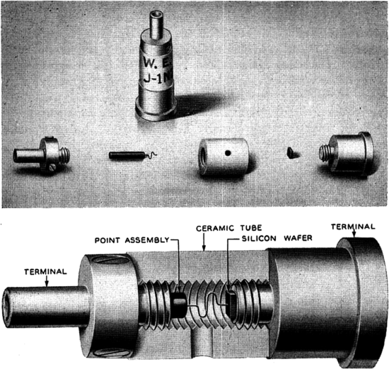
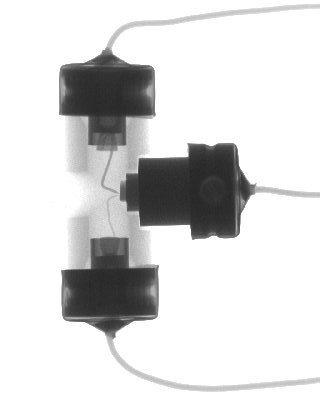
Further experimentation showed that the electrolyte was not needed: simply placing two point contacts very close together on the germanium surface sufficed to allow the current from one to modulate the current through the other. To achieve a very close spacing, Brattain wrapped a piece of thin gold foil around a triangular piece of plastic, then carefully slit the foil open at the tip. He then used a spring to press the whole triangle against the germanium, causing the two cut edges to touch the surface about two thousandths of an inch apart. This gave Bell Labs’ prototype transistor its signature look:
Like Mataré and Welker’s device, this was more or less a classic “cat’s whisker”, but with two point contacts instead of one. On December 16th, it generated significant power and voltage gain, at 1000 cycles, well within the audible range. A week later, with minor refinements, Bardeen and Brattain achieved 100x voltage gain and 40x power gain, and demonstrated to Bell executives that their device could reproduce audible speech.14 John Pierce, another member of the solid-state group, coined the term transistor as a riff on Bell’s name for the copper-oxide rectifier, the varistor.10
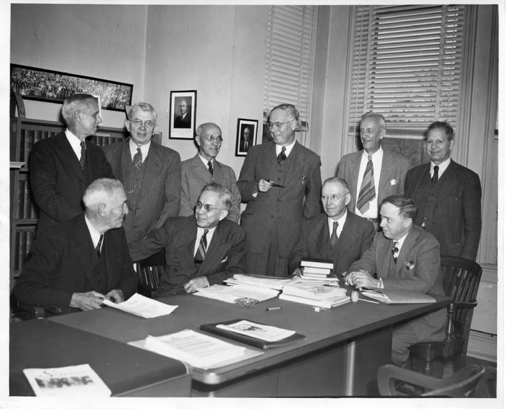
Bell kept their new creation under wraps for the next six months. They wanted to ensure they had a head start in realizing the commercial possibilities of the transistor before anyone else got their hands on it. The press conference was set for June 30, 1948, just in time to shatter any dreams of immortality that Welker and Mataré may have harbored. In the meantime the semiconductor group quietly tore itself apart. For as soon as he heard about Bardeen and Brattain’s achievement, their boss, Bill Shockley, began working to ensure that he would get the credit for it. Though he had played only a supervisory role, in all the announcement publicity Shockley got equal if not higher billing – as is clear from this publicity shot, which puts him in the center and at the lab bench:

But equal credit was not good enough for Shockley. So, even before anyone outside Bell knew of the transistor, he set about reinventing it, to make it his own. It was only the first of many such reinventions.
Further Reading
Robert Buderi, The Invention That Changed the World (1996)
Michael Riordan, “How Europe Missed the Transistor,” IEEE Spectrum (Nov. 1, 2005)
Michael Riordan and Lillian Hoddeson, Crystal Fire (1997)
Armand Van Dormael, “The ‘French’ Transistor,” http://www.cdvandt.org/VanDormael.pdf (1994)
- Marconi himself believed that the radio waves hugged the curvature of the Earth, but this theory had no backing from physicists. ↩
- Oswald G. Villard, “The Ionospheric Sounder and its Place in the History of Radio Science,” Radio Science, November 1976. I use the term radar as a convenience throughout, but that name actually originated only in 1940, when the U.S. Navy coined the term, as a shorthand for “RAdio Detection And Ranging.” ↩
- Radar thus followed the opposite course of the telescope, which was invented first for terrestrial military applications, and then shortly thereafter turned towards the heavens. ↩
- Buderi, 48. ↩
- This was intended to mislead foreign spies into believing it was investigating radioactivity, at a time when few thought that it could be effectively weaponized. ↩
- Buderi, 63-64. ↩
- The U.S. government investment in radar of course went well beyond the Rad Lab. Direct research investments aside, it purchased over a million radar sets during the war, at a total cost of about three billion dollars. By comparison, the Manhattan Project is estimated to have cost about two billion dollars. (https://en.wikipedia.org/wiki/Manhattan_Project) ↩
- As with most of the story of semiconductors, the actual physics of the thing are beyond my understanding. ↩
- Buderi, 316 ↩
- Buderi, 117-118, 319-320 ↩ ↩
- As Bray said decades later, “[w]e were not looking for a device, We were interested in finding out. We were discovering phenomena and the phenomena were anomalous in terms of what we knew, which was not very much, and the thing was to try to figure out what was happening. …I wonder if we had found transistor action as such whether we would have exploited it or made a big deal of it afterward. …The atmosphere here was towards basic physics.” Paul Henriksen, “Oral History of Ralph Bray,” 14 May 1982 (https://www.aip.org/history-programs/niels-bohr-library/oral-histories/4533) ↩
- Riordan and Hoddeson, 111-112 ↩
- He also was yet another protégé of John Van Vleck, like Atanasoff and Brattain before him. Like Atanasoff’s, Bardeen and Shockley’s dissertations were extremely computationally intensive. They required using the quantum mechanical theory of semiconductor materials as defined by Alan Wilson to crank out the energy structure of actual materials using a Monroe desk calculator. By helping create the transistor, they (indirectly and unwittingly) contributed to the elimination of this burden from the lives of future graduate students. ↩
- Buderi, 331. ↩

[…] [Previous part] [Next part] […]
LikeLike
[…] https://technicshistory.wordpress.com/2018/02/28/the-transistor-part-2-out-of-the-crucible/ […]
LikeLike
I eagerly look forward to every chapter in this history. Thank you again!
LikeLike
[…] [Previous part] […]
LikeLike
Like the first part, this was also equally interesting.
Very well presented.
I am purposely taking time to read these articles.
We know the history, but, not in such intricate details.
Great dedication with which the scientists involved worked.
Nice learning.
LikeLike